The sun's energy can be harnessed as either light or heat. The process of converting light (photons) to electricity (voltage) is called the photovoltaic (PV) effect. The PV effect was first discovered by the French physicist Edmund Becquerel in 1839 using copper oxide in an electrolyte. We'll go into more detail about the current materials for PV further down the page.
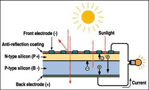
To create the PV effect, radiation from the sun ('sunlight') hits a photovoltaic cell. These cells are made up of two layers of semi-conducting material, typically silicon, that have been chemically treated. The industry refers to these layers as P and N. The boundary between P and N acts as a diode allowing electrons to move from N to P, but not from P to N. When photons with sufficient energy hit the cell, they cause electrons to move (from N to P only) causing excess electrons in the N-layer and a shortage in the P layer.
This voltage difference is typically in the range of 0.5V for as long as the cell is in sunlight. If you short-circuit the upper and lower layer a current runs of about 3 Amps. If you arrange sufficient cells in series, the result is a PV module or PV panel. Let's say 36 cells in series produce 36 x 0.5V = 18V at 3 Amps = 54Watts.
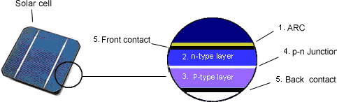
The following graphic sets out the layers within the cell. The top layer is an Anti-Reflective-Coating (ARC) that enhances the light effect of the sun. The N layer is typically semi-conducting silicon doped with phosphorus that creates the free flow of electrons. The P layer is again typically semi-conducting silicon, but this time doped with boron which creates the free flow of positive charges called “holes”. As the holes and electrons are attracted and move towards each other, they create an electrical field across the P-N junction. Sunlight striking this electrical field separates the electrons and holes, creating the voltage.
The voltage pushes the flow of electrons or 'DC current' to contacts at the front and back of the cell where it is conducted away along the wiring circuitry that connects the cells together.
Solar Cells and Arrays
Solar cells are typically combined into modules that hold about 40 cells; about 10 of these modules are mounted in PV arrays that can measure up to several meters on a side. These flat-plate PV arrays can be mounted at a fixed angle facing south, or they can be mounted on a tracking device that follows the sun, allowing them to capture the most sunlight over the course of a day. About 10 to 20 PV arrays can provide enough power for a household; for large electric utility or industrial applications, hundreds of arrays can be interconnected to form a single, large PV system.
Thin film solar cells use layers of semiconductor materials only a few micrometers thick. Thin film technology has made it possible for solar cells to now double as rooftop shingles, roof tiles, building facades, or the glazing for skylights or atria. The solar cell version of items such as shingles offer the same protection and durability as ordinary asphalt shingles.
Some solar cells are designed to operate with concentrated sunlight. These cells are built into concentrating collectors that use a lens to focus the sunlight onto the cells. This approach has both advantages and disadvantages compared with flat-plate PV arrays. The main idea is to use very little of the expensive semiconducting PV material while collecting as much sunlight as possible. But because the lenses must be pointed at the sun, the use of concentrating collectors is limited to the sunniest parts of the country.
Efficiency
The performance of a solar cell is measured in terms of its efficiency at turning sunlight into electricity. Only sunlight of certain energies will work efficiently to create electricity, and much of it is reflected or absorbed by the material that make up the cell. Because of this, a typical commercial solar cell has an efficiency of 15%-about one-sixth of the sunlight striking the cell generates electricity, although leading competitors are working towards 18%. The theoretical maximum efficiency of a solar cell using current techniques is in the 30% range
For this reason, implementations of photovoltaics are most effective in areas with a large amount of daily sunlight. Note that the solar cells are temperature-dependent, such that in a cold environment a photovoltaic cell performs better than in a hot environment. (0.3% increase per 1 degree C drop in temperature). Unfortunately, there aren't a lot of places on earth that are both cold and have long sunny days.
Low efficiencies mean that larger arrays are needed, and that means higher cost. Improving solar cell efficiencies while holding down the cost per cell is an important goal of the all participants in the solar energy industry, and they have made significant progress. The first solar cells, built in the 1950s, had efficiencies of less than 4%.
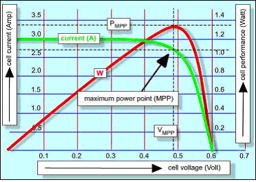
The diagram on the left is sets out the maximum power performance of a photovoltaic cell. The red curve is the voltage-performance graph of the cell and the green curve is the current-voltage graph. The best performance (in Watts) is obtained at that voltage at which the current definitely starts to decline: the maximum power point (MPP).
PV materials– Silicon and Thin Film technologies
Three key elements in a solar cell form the basis of their manufacturing technology. The first is the semiconductor, which absorbs light and converts it into electron-hole pairs. The second is the semiconductor junction, which separates the photo-generated carriers (electrons and holes), and the third is the contacts on the front and back of the cell that allow the current to flow to the external circuit. The two main categories of technology are defined by the choice of the semiconductor: either crystalline silicon in a wafer form or thin films of other materials.
Crystalline Silicon cells: Crystalline silicon solar cells currently represent over 90% of the world market for solar cells. Historically, crystalline silicon (c-Si) has been used as the light-absorbing semiconductor in most solar cells, even though it is a relatively poor absorber of light and requires a considerable thickness (several hundred microns) of material. Nevertheless, it has proved convenient because it yields stable solar cells with good efficiencies (11-16%, half to two-thirds of the theoretical maximum) and uses process technology developed from the huge knowledge base of the microelectronics industry.
Two types of crystalline silicon are used in the industry. The first is monocrystalline, produced by slicing wafers (up to 150mm diameter and 350 microns thick) from a high-purity single crystal boule. The second is multicrystalline silicon, made by sawing a cast block of silicon first into bars and then wafers. The main trend in crystalline silicon cell manufacture is toward multicrystalline technology. Monocrystalline cells have higher conversion efficiency than multicrystalline cells, but costs of monocrystalline wafers are generally higher than multicrystalline wafers.
For both mono- and multicrystalline Si, a semiconductor homojunction is formed by diffusing phosphorus (an n-type dopant) into the top surface of the boron doped (p-type) Si wafer. Screen-printed contacts are applied to the front and rear of the cell, with the front contact pattern specially designed to allow maximum light exposure of the Si material with minimum electrical (resistive) losses in the cell.
The most efficient production cells use monocrystalline c-Si with laser grooved, buried grid contacts for maximum light absorption and current collection.
Some companies are using technologies that by-pass some of the inefficiencies of the crystal growth/casting and wafer sawing route. One route is to grow a ribbon of silicon, either as a plain two-dimensional strip or as an octagonal column, by pulling it from a silicon melt.
Another is to melt silicon powder on a cheap conducting substrate. These processes may bring with them other issues of lower growth/pulling rates and poorer uniformity and surface roughness.
Each c-Si cell generates about 0.5V, so 36 cells are usually soldered together in series to produce a module with an output to charge a 12V battery. The cells are hermetically sealed under toughened, high transmission glass to produce highly reliable, weather resistant modules.
Thin film solar cells represent a small, but fast growing segment of the PV market. The high cost of crystalline silicon wafers (they make up 40-50% of the cost of a finished module) has led the industry to look at cheaper materials to make solar cells.
The selected materials are all strong light absorbers and only need to be about 1micron thick, so materials costs are significantly reduced. The most common materials are amorphous silicon (a-Si, still silicon, but in a different form), or the polycrystalline materials: cadmium telluride (CdTe) and copper indium (gallium) diselenide (CIS or CIGS).
Each of these three is amenable to large area deposition (on to substrates of about 1 meter dimensions) and hence high volume manufacturing. The thin film semiconductor layers are deposited on to either coated glass or stainless steel sheet.
The semiconductor junctions are formed in different ways, either as a p-i-n device in amorphous silicon, or as a hetero-junction (e.g. with a thin cadmium sulphide layer) for CdTe and CIS. A transparent conducting oxide layer (such as tin oxide) forms the front electrical contact of the cell, and a metal layer forms the rear contact.
Thin film technologies are all complex. They have taken at least twenty years, supported in some cases by major corporations, to get from the stage of promising research (about 8% efficiency at 1cm2 scale) to the first manufacturing plants producing early product.
Amorphous silicon is the most well developed of the thin film technologies. In its simplest form, the cell structure has a single sequence of p-i-n layers. Such cells suffer from significant degradation in their power output (in the range 15-35%) when exposed to the sun.
The mechanism of degradation is called the Staebler-Wronski Effect, after its discoverers. Better stability requires the use of a thinner layers in order to increase the electric field strength across the material. However, this reduces light absorption and hence cell efficiency.
This has led the industry to develop tandem and even triple layer devices that contain p-i-n cells stacked one on top of the other. In the cell at the base of the structure, the a-Si is sometimes alloyed with germanium to reduce its band gap and further improve light absorption. All this added complexity has a downside though; the processes are more complex and process yields are likely to be lower.
In order to build up a practically useful voltage from thin film cells, their manufacture usually includes a laser scribing sequence that enables the front and back of adjacent cells to be directly interconnected in series, with no need for further solder connection between cells.
As before, thin film cells are laminated to produce a weather resistant and environmentally robust module. Although they are less efficient (production modules range from 5 to 8%), thin films are potentially cheaper than c-Si because of their lower materials costs and larger substrate size.
However, some thin film materials have shown degradation of performance over time and stabilized efficiencies can be 15-35% lower than initial values. Many thin film technologies have demonstrated best cell efficiencies at research scale above 13%, and best prototype module efficiencies above 10%. The technology that is most successful in achieving low manufacturing costs in the long run is likely to be the one that can deliver the highest stable efficiencies (probably at least 10%) with the highest process yields.
Amorphous silicon is the most well-developed thin film technology to-date and has an interesting avenue of further development through the use of "microcrystalline" silicon which seeks to combine the stable high efficiencies of crystalline Si technology with the simpler and cheaper large area deposition technology of amorphous silicon.
However, conventional c-Si manufacturing technology has continued its steady improvement year by year and its production costs are still falling too.
Solar Energy Engineering |
Why Solar Energy? |
Solar Electricity |
Passive Solar Systems & Solar Hot Water